Recent Advances in 3D Chip Stacking and Advanced Packaging Technologies

Aug 26, 2025 By

The relentless pursuit of miniaturization and performance in the semiconductor industry has entered a new, three-dimensional phase. For decades, the guiding principle was Moore's Law, the observation that the number of transistors on a microchip doubles about every two years, achieved primarily by shrinking transistor sizes on a flat, two-dimensional plane of silicon. However, as we approach the physical and economic limits of this scaling, the industry's focus has dramatically shifted upwards. The new frontier is not just making things smaller, but stacking them. 3D chip stacking and advanced packaging technologies have moved from niche applications to the central strategy for continuing the pace of innovation, promising to redefine the very architecture of computing for the AI era and beyond.

The concept of stacking chips is not entirely new, but its implementation has evolved from simple memory dies in a single package to highly complex, heterogeneous systems. The fundamental driver is the growing inefficiency of the traditional monolithic system-on-chip (SoC). As these chips have grown larger to accommodate more functions, the physical distance that signals must travel between different components, like the CPU cores and memory, has increased. This distance, known as the interconnect delay, becomes a significant bottleneck for speed and power consumption. By stacking chips vertically and connecting them with thousands of ultra-short, vertical interconnects, this delay is slashed. Data can move between functional blocks at unprecedented speeds and with far less energy, a critical advantage for data-intensive applications like artificial intelligence, high-performance computing, and 5G networking.

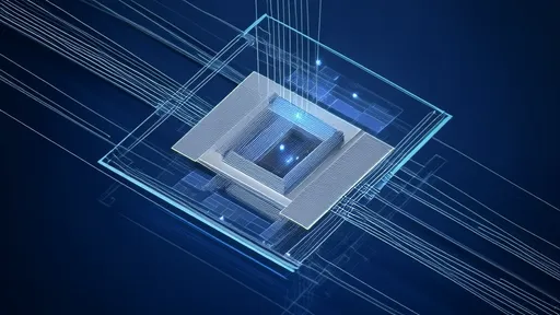
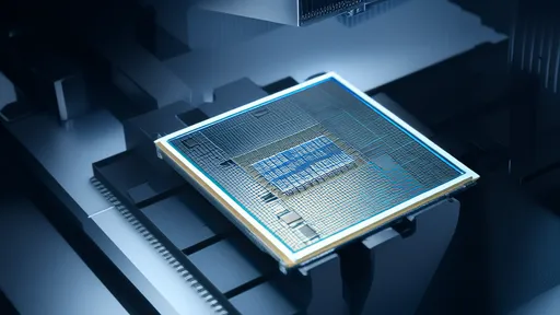
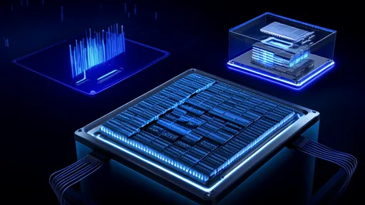
At the heart of this 3D revolution are several key enabling technologies. Through-Silicon Vias (TSVs) are the microscopic vertical conduits that electrically connect a stack of dies. Creating these involves etching deep, narrow holes through the silicon wafer, lining them with an insulating layer, and filling them with a conductive material like copper. The development of high-aspect-ratio TSVs—incredibly deep yet narrow—has been a monumental engineering achievement, allowing for a massive density of connections without compromising the structural integrity of the silicon. Alongside TSVs, hybrid bonding has emerged as a game-changer. Unlike older techniques that used solder bumps to connect dies, hybrid bonding directly fuses the copper interconnects on the surface of two dies with a dielectric material, creating a permanent, atomic-level bond. This process enables an order-of-magnitude increase in connection density and allows for finer pitches, meaning more connections in a smaller area, which is essential for achieving the bandwidth demands of tomorrow's chips.

The industry is no longer just stacking identical memory chips. The most powerful trend is heterogeneous integration, where fundamentally different types of chips, often manufactured on different process nodes optimized for their specific function, are integrated into a single package. Imagine a system where a high-performance logic chip built on the latest 3nm process is stacked atop a specialized analog/RF chip made on a older, more cost-effective 28nm node, with a high-bandwidth memory (HBM) cube sitting right beside them, all connected through a sophisticated silicon interposer. This "mix-and-match" approach allows designers to break free from the constraints of a one-size-fits-all manufacturing process. They can optimize each component for performance, power, and cost, and then integrate them into a system that performs as if it were a single chip. This is the architectural shift enabling the specialized accelerators that power modern AI and machine learning workloads.

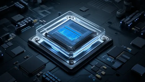
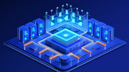
The role of the package itself has been utterly transformed. It is no longer a simple protective shell with pins to connect to a circuit board; it has become an active platform for integration—a system-in-package (SiP). Silicon interposers, passive slices of silicon embedded with a dense network of wiring, act as a miniature motherboard within the package, routing signals between chiplets with high efficiency. Even more advanced are embedded silicon bridge technologies, where small pieces of silicon with ultra-dense interconnect routes are embedded within the package substrate to connect chiplets over very short distances. On the horizon, glass substrates are being researched as a successor to organic substrates and silicon interposers. Glass offers superior flatness, thermal and mechanical stability, and the potential for even finer wiring, which could support an even greater number of connections for future 3D architectures.

The implications of these advancements are profound and are already being felt across the technology landscape. In artificial intelligence, the ability to place vast pools of high-bandwidth memory immediately adjacent to AI accelerator cores is eliminating the memory bottleneck that has constrained model size and training times. This co-packaged architecture is what allows for the trillion-parameter models that are pushing the boundaries of what AI can do. In data centers, CPUs are increasingly being designed as collections of smaller "chiplets" rather than a single large die. These chiplets, which might include compute cores, I/O interfaces, and cache memory, can be tested separately and then integrated using advanced packaging, improving manufacturing yield and allowing for more modular and scalable server designs. For consumer devices, these technologies enable the sleek, powerful gadgets we use daily, allowing for more functionality to be packed into a smaller form factor without sacrificing battery life.

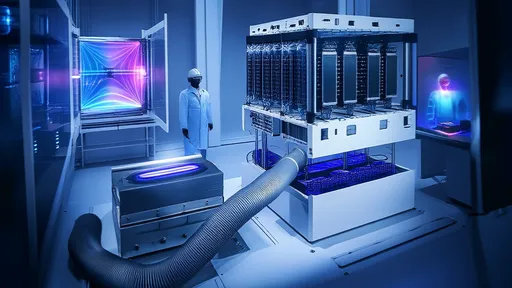
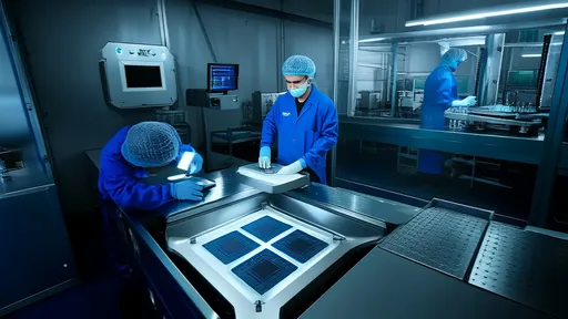
Despite the tremendous progress, significant challenges remain on the path to ubiquitous 3D integration. Thermal management is perhaps the most daunting. Stacking power-hungry chips creates a high power density, turning these packages into miniature ovens. Dissipating this heat effectively to prevent performance throttling or damage requires innovative cooling solutions, from advanced thermal interface materials and heat spreaders to integrated microfluidic channels that pump coolant directly through the stack. Testing and yield present another complex puzzle. Testing a fully assembled 3D stack is exceedingly difficult if an underlying die is found to be faulty. Strategies like known-good-die (KGD) testing, where each die is rigorously tested before assembly, and built-in self-test (BIST) circuits are critical but add cost and complexity. Furthermore, the design tools and electronic design automation (EDA) software needed to architect these complex 3D systems are still maturing, requiring a new generation of tools that can handle the multi-physics challenges of thermal, mechanical, and electrical co-design.

Looking forward, the trajectory of 3D integration points toward even greater intimacy between components. We are moving from 3D packaging, where fully fabricated chips are stacked, to true 3D monolithic integration, where transistor layers are built directly on top of each other on a single wafer. This nascent technology, often called sequential integration, could eventually lead to systems with logic transistors stacked over memory cells, creating an unparalleled level of performance and efficiency. The industry is also exploring the integration of non-silicon elements, such as photonics, for light-speed data movement within the package, and the inclusion of sensors and micro-electromechanical systems (MEMS) to create complete sensing and computing systems on a chip. The package is becoming the new motherboard, the new server rack, and the new city planner for the world of computing, orchestrating the flow of data in three dimensions.

In conclusion, the era of simply scaling down transistors on a flat plane is giving way to a more sophisticated, multi-dimensional approach. 3D chip stacking and advanced packaging are not merely incremental improvements; they represent a fundamental paradigm shift in semiconductor design and manufacturing. By building up rather than just scaling down, the industry is overcoming the limitations of Moore's Law and paving the way for a new generation of powerful, efficient, and highly specialized computing systems. This vertical revolution is building the foundation for the next decade of technological innovation, from pervasive AI and the metaverse to discoveries in genomics and materials science that we have yet to imagine.

Recommend Posts
IT

Greening 5G Networks: Enhancing Energy Efficiency with KPIs

By /Aug 26, 2025

The global rollout of 5G networks represents one of the most significant technological shifts of our generation, promising unprecedented speed, connectivity, and the foundation for a fully realized Internet of Things. However, this massive infrastructure expansion comes with a substantial energy cost, raising critical questions about its environmental impact. As data traffic is projected to grow exponentially, the telecommunications industry faces a pressing challenge: how to deliver these advanced services while simultaneously reducing its carbon footprint and operating expenses. The pursuit of a greener 5G network is no longer a niche concern but a central pillar of corporate strategy and environmental responsibility.
IT

Near-Memory Computing Technology to Alleviate Data Transfer Bottlenecks

By /Aug 26, 2025

The relentless pursuit of computational speed has long been a defining feature of the technology industry. For decades, this pursuit was largely satisfied by the predictable cadence of Moore's Law, which delivered ever-increasing numbers of transistors on a single chip, allowing processors to execute instructions at breathtaking speeds. However, a fundamental and increasingly critical imbalance has emerged, casting a long shadow over these advancements. The core of the problem is not the speed of computation itself, but the agonizingly slow and power-hungry process of moving the data needed for those computations. This is the infamous "data movement bottleneck," a wall that traditional computing architectures are repeatedly crashing into.
IT

Cyber Digital Twin: Simulating and Optimizing Physical Networks in the Virtual World

By /Aug 26, 2025

In the rapidly evolving landscape of digital transformation, one concept is steadily gaining traction for its profound implications across industries: network digital twins. This technology, which creates virtual replicas of physical networks, is not merely a buzzword but a pivotal innovation reshaping how organizations design, manage, and optimize complex systems. By mirroring real-world networks in a dynamic digital environment, digital twins enable unprecedented levels of simulation, analysis, and prediction, offering a gateway to enhanced efficiency, reliability, and innovation.
IT

In-Memory Computing" Architecture Breaks the "Memory Wall"

By /Aug 26, 2025

The relentless pursuit of computational efficiency has long been haunted by a formidable bottleneck known as the "memory wall." This term describes the critical performance limitation that arises from the physical separation between the central processing unit (CPU) and main memory in conventional von Neumann architectures. Data must constantly shuttle back and forth across this divide, a process that consumes immense amounts of time and energy. As processors have become exponentially faster, this data movement has emerged as the dominant constraint, throttling system performance and inflating power consumption, particularly for data-intensive workloads like artificial intelligence and big data analytics.
IT

A Comprehensive Guide to Designing, Deploying, and Maintaining Liquid-Cooled Data Centers

By /Aug 26, 2025

The hum of cooling fans has long been the defining soundtrack of data centers worldwide. For decades, air cooling has been the default, the comfortable and well-understood method for managing the immense thermal output of computing equipment. But as computational demands skyrocket—driven by artificial intelligence, high-performance computing, and ever-denser server architectures—the limitations of moving air have become starkly apparent. We are rapidly approaching a thermal ceiling, a point where air can no longer carry away heat efficiently enough. In this new era, the industry is turning to a more fundamental and powerful medium: liquid. The transition to liquid cooling is not merely an incremental upgrade; it represents a fundamental paradigm shift in data center design, deployment, and operational philosophy.
IT

Sustainable Data Centers: Practices of Waste Heat Recovery and Renewable Energy Utilization

By /Aug 26, 2025

As the digital age accelerates, data centers have become the backbone of modern infrastructure, powering everything from cloud computing to artificial intelligence. However, this growth comes with a significant environmental cost, primarily due to their massive energy consumption. In response, the industry is increasingly focusing on sustainable practices, with two key strategies emerging: waste heat recovery and the integration of renewable energy sources. These approaches not only reduce the carbon footprint of data centers but also enhance operational efficiency and economic viability.
IT

Integration of Satellite Internet (Starlink, etc.) with Traditional Telecommunication Networks

By /Aug 26, 2025

The telecommunications landscape is undergoing a profound transformation, driven by the convergence of two historically distinct domains: terrestrial networks and non-terrestrial, or satellite, networks. For decades, these systems operated in parallel, serving different markets and use cases with minimal interaction. However, the advent of advanced Low Earth Orbit (LEO) satellite constellations, most notably SpaceX's Starlink, is shattering this long-standing paradigm. We are now witnessing the early stages of a deep and complex integration, a fusion that promises to create a seamless, resilient, and truly global network fabric, fundamentally altering how humanity connects.
IT

How Wi-Fi 7's MLO (Multi-Link Operation) Technology Completely Transforms the Wireless Experience

By /Aug 26, 2025

The wireless landscape stands on the brink of its most profound transformation in over a decade, ushered in by the arrival of Wi-Fi 7 and its cornerstone innovation: Multi-Link Operation, or MLO. This is not merely an incremental speed boost or a slight extension of range. MLO represents a fundamental architectural shift in how Wi-Fi devices communicate, promising to dismantle long-standing limitations and finally deliver on the full, seamless potential of wireless connectivity. For years, users have accepted the trade-offs—the dropped video call when moving between rooms, the laggy game session when others stream Netflix, the frustrating wait for large files to transfer. Wi-Fi 7 with MLO is engineered to make these compromises a relic of the past.
IT

New Breakthrough in Optical Communication Technology: Single-Wave Rate Approaches 1.6Tb/s

By /Aug 26, 2025

The telecommunications landscape is undergoing a seismic shift, driven by an insatiable global demand for data. In laboratories and R&D centers worldwide, the race to push the boundaries of data transmission speed has reached a new, staggering milestone: the successful demonstration of single-carrier data transmission at 1.6 Terabits per second (Tb/s). This is not merely an incremental step; it is a quantum leap that promises to redefine the very backbone of our digital infrastructure, from hyper-scale data centers to the transoceanic cables that connect continents.
IT

Terahertz Communications: A Potential Key Technology for Future 6G

By /Aug 26, 2025

The race toward 6G is already underway, and while it may seem like a distant future given the ongoing global rollout of 5G, researchers and industry leaders are intensely exploring the technologies that will define the next generation of wireless communication. Among the most promising and revolutionary candidates is terahertz (THz) communication, operating in the frequency range of 0.1 to 10 THz. This largely untapped region of the electromagnetic spectrum holds the key to unlocking unprecedented data rates and capacities, potentially revolutionizing how we connect, compute, and interact with the digital world.
IT

Recent Advances in 3D Chip Stacking and Advanced Packaging Technologies

By /Aug 26, 2025

The relentless pursuit of miniaturization and performance in the semiconductor industry has entered a new, three-dimensional phase. For decades, the guiding principle was Moore's Law, the observation that the number of transistors on a microchip doubles about every two years, achieved primarily by shrinking transistor sizes on a flat, two-dimensional plane of silicon. However, as we approach the physical and economic limits of this scaling, the industry's focus has dramatically shifted upwards. The new frontier is not just making things smaller, but stacking them. 3D chip stacking and advanced packaging technologies have moved from niche applications to the central strategy for continuing the pace of innovation, promising to redefine the very architecture of computing for the AI era and beyond.
IT

Quantum Computing Hardware Roadmap: Which Will Take the Lead - Superconducting, Ion Trap, or Photonic?

By /Aug 26, 2025

The race for quantum computing supremacy has entered a fascinating phase, with three distinct hardware approaches—superconducting qubits, trapped ions, and photonic systems—vying for dominance. Each path carries its own philosophical and engineering challenges, reflecting divergent schools of thought about how to tame the quantum world. Unlike classical computing’s relatively linear evolution, the quantum hardware landscape resembles a multidimensional chessboard where progress in one area often reshapes the entire competitive field.
IT

Convergence of Software-Defined Wide Area Network (SD-WAN) and Secure Access Service Edge (SASE)

By /Aug 26, 2025

The convergence of Software-Defined Wide Area Networking (SD-WAN) and Secure Access Service Edge (SASE) represents a pivotal shift in how enterprises architect their network and security infrastructures. As digital transformation accelerates and remote work becomes ubiquitous, organizations are grappling with the limitations of traditional network models. The legacy approach of backhauling traffic to centralized data centers for security inspection is no longer tenable in an era where cloud applications and distributed users demand low-latency, secure access from anywhere. This has set the stage for the natural marriage of SD-WAN's agile connectivity and SASE's comprehensive security framework, creating a unified cloud-native architecture that is reshaping the future of enterprise networking.
IT

Ecosystem Progress of RISC-V in Server and High-Performance Computing Fields

By /Aug 26, 2025

The RISC-V architecture, once perceived as a niche player in the embedded and IoT spaces, is now making significant inroads into the demanding realms of servers and high-performance computing (HPC). This progression from the periphery to the potential mainstream of computational heavy-lifting is not a sudden leap but the result of a meticulously growing, albeit complex, ecosystem. The narrative is no longer about if RISC-V can compete in these markets, but how and when it will establish a formidable presence.
IT

Deterministic Networking in Industrial Automation Applications

By /Aug 26, 2025

Industrial automation stands at the cusp of a transformative era, driven by the relentless demand for higher efficiency, precision, and reliability. In environments where a millisecond delay can cascade into significant operational failures or safety hazards, the quality of network communication is not merely a technical detail—it is the backbone of entire production ecosystems. Traditional best-effort IP networks, while revolutionary in general computing and internet services, fall critically short in these high-stakes scenarios. Their inherent unpredictability in latency, jitter, and packet loss creates a fundamental barrier to achieving the seamless, synchronized control required by modern industrial applications such as motion control, robotic assembly lines, and process automation.
IT

How DPU/IPU Reconstructs Cloud Computing Data Center Architecture

By /Aug 26, 2025

The data center landscape is undergoing a seismic shift, driven by an insatiable demand for computational power, lower latency, and more efficient resource utilization. At the heart of this transformation lies a new class of hardware: the SmartNIC, also known as a Data Processing Unit (DPU) or Infrastructure Processing Unit (IPU). These are not mere network interface cards; they are powerful, specialized computers-on-a-card that are fundamentally rearchitecting the very foundations of cloud computing data centers.
IT

Technology Selection between Cellular Networks (4G/5G) and IoT Private Networks (LoRa, NB-IoT)

By /Aug 26, 2025

In the rapidly evolving landscape of wireless communication, the choice between cellular networks like 4G and 5G and specialized Internet of Things (IoT) networks such as LoRa (Long Range) and NB-IoT (Narrowband IoT) has become a critical decision for businesses and developers. Each technology offers distinct advantages and trade-offs, making the selection process highly dependent on specific application requirements, including range, bandwidth, power consumption, and cost. Understanding the nuances of these technologies is essential for deploying efficient, scalable, and future-proof IoT solutions.
IT

The Commercialization Process and Challenges of Silicon Photonics

By /Aug 26, 2025

The commercialization of silicon photonics represents one of the most significant technological shifts in the semiconductor and telecommunications industries in recent decades. Born from the marriage of silicon semiconductor fabrication and photonic principles, this technology promises to address the growing demands for faster, more efficient data transmission in an increasingly connected world. While the theoretical groundwork was laid as far back as the 1980s, it is only in the last ten to fifteen years that we have witnessed a concerted push to transition these devices from research labs to high-volume manufacturing facilities. The journey, however, is far from straightforward, presenting a complex tapestry of engineering triumphs and persistent, formidable challenges.
IT

Optimizing Distributed Storage with Next-Generation NVMe-over-Fabric Technology

By /Aug 26, 2025

The storage industry stands at the precipice of a transformative shift, driven by the relentless demand for higher performance, lower latency, and greater scalability in data centers. At the heart of this evolution lies NVMe-over-Fabrics (NVMe-oF), a technology that is fundamentally rearchitecting how we think about and deploy distributed storage systems. By extending the revolutionary benefits of Non-Volatile Memory Express (NVMe) across network fabrics, it promises to eliminate the bottlenecks that have long plagued traditional storage area networks (SANs) and network-attached storage (NAS) architectures.
IT

Platform Engineering: Enhancing Developer Experience and Efficiency

By /Aug 26, 2025

In the ever-evolving landscape of software development, a transformative shift is underway as organizations increasingly embrace platform engineering to redefine how development teams operate. This discipline, focused on building and maintaining internal developer platforms (IDPs), is rapidly becoming a cornerstone of modern tech strategy. By abstracting infrastructure complexities and providing self-service capabilities, platform engineering empowers developers to focus on what they do best—writing code and delivering business value—rather than wrestling with deployment pipelines and cloud configurations.