The commercialization of silicon photonics represents one of the most significant technological shifts in the semiconductor and telecommunications industries in recent decades. Born from the marriage of silicon semiconductor fabrication and photonic principles, this technology promises to address the growing demands for faster, more efficient data transmission in an increasingly connected world. While the theoretical groundwork was laid as far back as the 1980s, it is only in the last ten to fifteen years that we have witnessed a concerted push to transition these devices from research labs to high-volume manufacturing facilities. The journey, however, is far from straightforward, presenting a complex tapestry of engineering triumphs and persistent, formidable challenges.
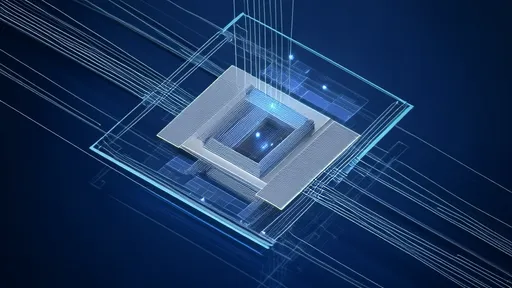
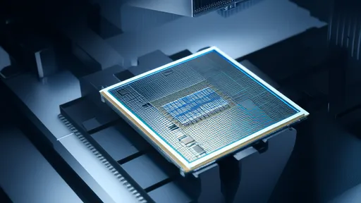
At its core, silicon photonics leverages the well-established and highly sophisticated infrastructure of the complementary metal-oxide-semiconductor (CMOS) industry. The fundamental premise is elegant: use light instead of, or in conjunction with, electrical signals to transmit data. By fabricating optical components like waveguides, modulators, and photodetectors directly onto a silicon substrate, manufacturers can theoretically produce high-performance, integrated photonic circuits at a scale and cost that traditional materials like indium phosphide or lithium niobate could never achieve. The potential applications are vast, spanning data centers and high-performance computing, telecommunications, medical sensing, and the nascent field of LiDAR for autonomous vehicles. The promise of overcoming the bandwidth and power limitations of copper interconnects has made silicon photonics a critical area of investment for tech giants and startups alike.
The data center has emerged as the primary battleground and the most compelling use case for early commercial adoption. As cloud computing, artificial intelligence, and big data analytics drive an exponential increase in data traffic, the physical limitations of electrical cabling within and between server racks have become a critical bottleneck. Electrical interconnects consume significant power, generate substantial heat, and face bandwidth-distance constraints. Silicon photonics offers a path forward. Integrated transceivers that convert electrical signals to optical signals and back again are now being deployed to create faster, more energy-efficient links. These optical engines are enabling data rates of 400 gigabits per second and beyond, forming the backbone of next-generation data center architectures. Companies like Intel, Cisco, and numerous specialized firms are already shipping products in volume, signaling that the technology has firmly moved beyond a niche novelty.
Despite these promising strides, the path to widespread commercialization is littered with technical and economic hurdles. One of the most significant challenges lies in the inherent material properties of silicon itself. While silicon is an excellent medium for guiding light, it is a poor emitter of light. Unlike direct bandgap materials that efficiently produce light, silicon is an indirect bandgap semiconductor, making it notoriously inefficient for building lasers. This has forced the industry to adopt hybrid integration approaches, where light-emitting materials like indium phosphide are bonded to the silicon photonic chip. This process of heterogeneous integration adds complexity, cost, and potential points of failure to the manufacturing workflow. Achieving high-yield, reliable attachment of these foreign materials to a silicon wafer remains a primary focus of research and development.
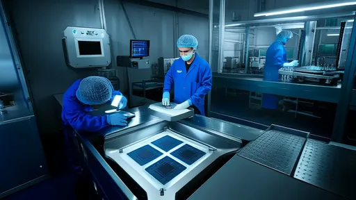
Furthermore, the packaging and testing of silicon photonic devices present a monumental challenge that often dwarfs the cost of the chip itself. Aligning microscopic optical fibers to nanoscale waveguides on the chip with sub-micron precision is an incredibly delicate and expensive process. It requires specialized equipment and a high degree of manual intervention, which stands in stark contrast to the highly automated, parallelized processes used in traditional electronic chip packaging. This "packaging bottleneck" threatens to undermine the cost advantages gained from using CMOS fabrication. The industry is actively pursuing solutions, including the development of standardized optical connectors, photonic wire bonding techniques, and more advanced passive alignment strategies to drive down these costs and enable true scalability.
Another layer of complexity is added by the need for co-packaged optics, an architecture that is gaining traction as a future solution. Instead of having optical transceivers plugged into the faceplate of a switch, the idea is to move the optical engines much closer to the switch's application-specific integrated circuit (ASIC), often on the same package substrate. This reduces power consumption, increases bandwidth density, and improves signal integrity. However, co-packaging introduces a new set of challenges related to thermal management, mechanical stress, and the integration of dissimilar materials and technologies. It requires unprecedented levels of collaboration between ASIC designers, photonic integrated circuit designers, and packaging experts, blurring the traditional boundaries between these disciplines.
On the economic front, the business landscape for silicon photonics is both vibrant and volatile. The market is currently a mix of large, vertically integrated semiconductor companies and a ecosystem of agile, focused startups. This diversity drives innovation but also creates a fragmented environment with competing proprietary standards and integration approaches. For end-users, this can lead to concerns about vendor lock-in and long-term supply stability. Moreover, the capital expenditure required to develop and scale manufacturing capabilities is enormous, creating a high barrier to entry. Many startups rely on partnerships with larger entities or foundry services to bring their designs to market, a dynamic that adds another layer of commercial complexity to the technical ones.
Looking ahead, the future of silicon photonics commercialization appears bright, albeit demanding. The relentless growth of data ensures that the underlying drivers for this technology will only intensify. Success will likely belong to those who can master the holistic integration of photonics and electronics, not just at the chip level, but at the system and packaging levels as well. Breakthroughs in areas like monolithically integrated light sources on silicon, whether through germanium tin alloys or other novel materials, could be a game-changer, potentially simplifying the manufacturing process dramatically. Furthermore, the maturation of design automation tools and the establishment of industry-wide standards and interoperable platforms will be crucial for reducing development costs and time-to-market.
In conclusion, the story of silicon photonics is still being written. It is a narrative of brilliant innovation constantly grappling with stubborn physical and economic realities. The technology has successfully navigated the treacherous path from academic concept to commercial product, finding its first major foothold in the world's data centers. Yet, the journey to becoming a ubiquitous, foundational technology on par with digital electronics is far from over. It will require continued investment, cross-disciplinary collaboration, and a sustained focus on solving the intricate problems of integration, packaging, and scalability. The companies and research institutions that can navigate this complex landscape will not only reap significant commercial rewards but will also help power the next evolution of our digital world.

By /Aug 26, 2025

By /Aug 26, 2025

By /Aug 26, 2025
By /Aug 26, 2025

By /Aug 26, 2025

By /Aug 26, 2025

By /Aug 26, 2025

By /Aug 26, 2025

By /Aug 26, 2025

By /Aug 26, 2025
By /Aug 26, 2025

By /Aug 26, 2025

By /Aug 26, 2025

By /Aug 26, 2025

By /Aug 26, 2025

By /Aug 26, 2025

By /Aug 26, 2025
By /Aug 26, 2025

By /Aug 26, 2025

By /Aug 26, 2025